Not on air · 2 of 3 networks checked
Chipmetrics
- chipmetrics.com
- Hardware & Electronics
- FI
- 10 employees
Chipmetrics’s ads on LinkedIn, Meta and Google, recorded by adsrunning. Browse the latest here for free. Sign up free to see all 33. Watch Chipmetrics with Starter to get each new one in your feed.
Watchlist with Starter · $49/mo
| Network | Status | Live ads | Nov 2025LinkedIn activity · 52 weeksOct 2026 | Checked | Next step |
|---|---|---|---|---|---|
| None recorded | 0 | Checked 30 Oct 2026 | See all 33 ads → | ||
| Meta | Not checked | — | |||
| None recorded | 0 | No ads found on the Google Ads Transparency Center | Checked 25 Oct 2026 | Collect them with the API → |
Chipmetrics has no live LinkedIn ads. We recorded no Google ads on 25 Oct 2026.
Latest ads
- LINKEDIN · IMAGESince 3 Apr 2026
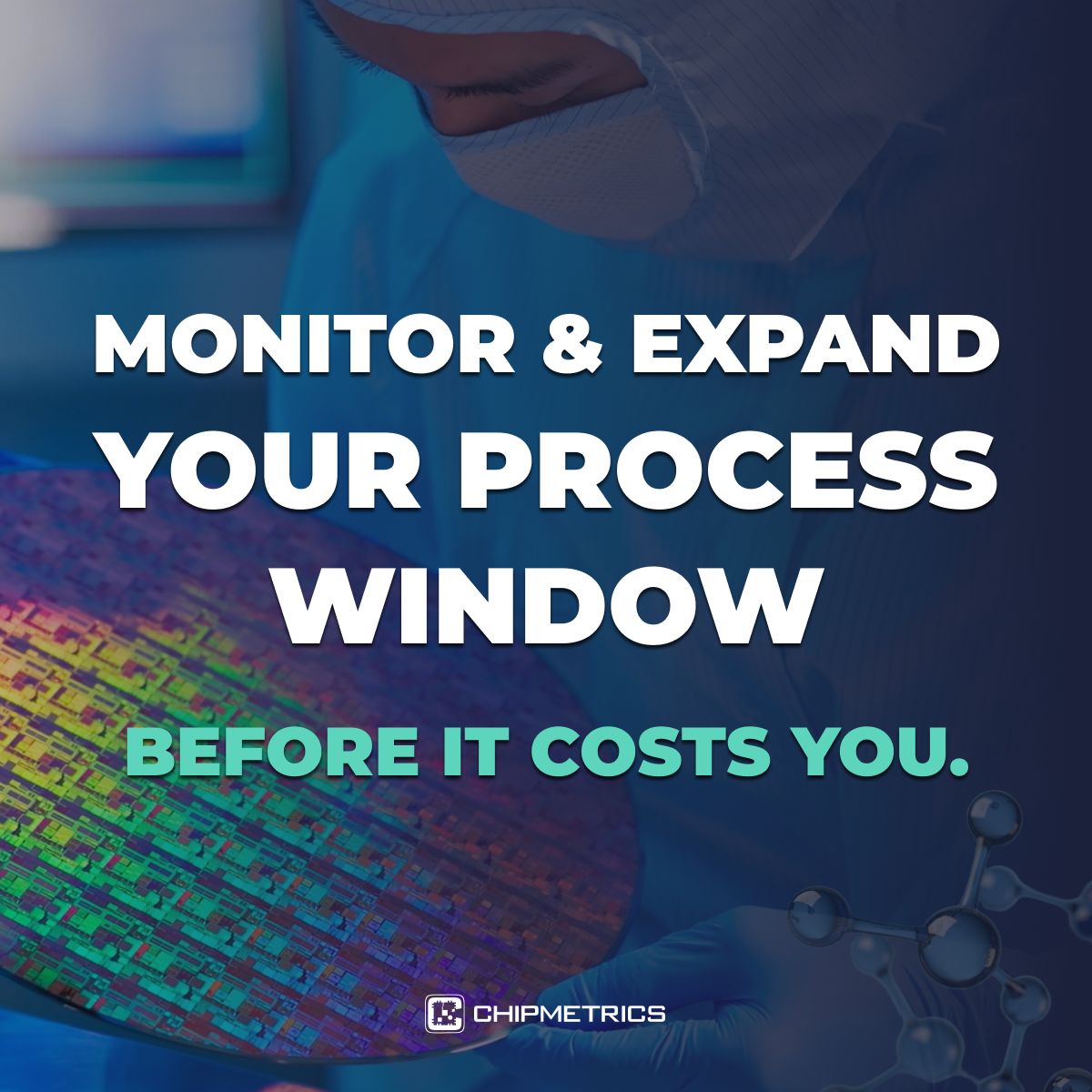
In modern semiconductor manufacturing, as device architectures push upward in aspect ratio (HAR/UHAR), the window of acceptable performance for thin film deposition becomes narrower. Tiny deviations in precursor diffusion, pulse timing, conformality, penetration depth, or substrate geometry can lead to yield loss, reliability issues, or process drift that is expensive to correct – once you've already committed wafers. With Chipmetrics, you can map, monitor, and expand your process window before it costs you. 👉 Ready to know your limits? 1) Request a demo of PillarHall® and VHAR1 test chips 2) Explore 300 mm pocket wafer strategies for fab-level monitoring 3) Send a sample for analysis Stop guessing. Start measuring. Define your process window with Chipmetrics.
- LINKEDIN · IMAGESince 3 Apr 2026
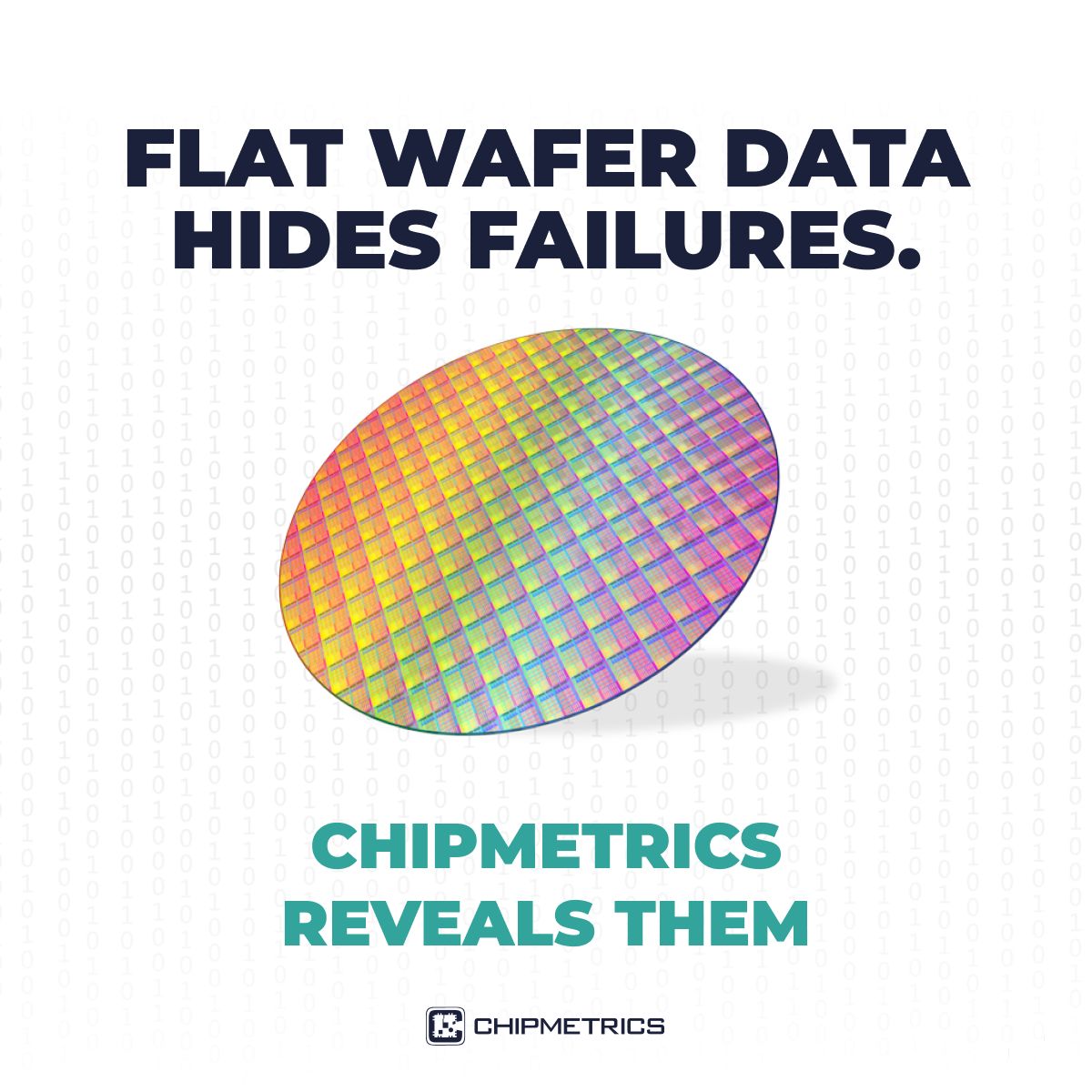
In modern semiconductor manufacturing, as device architectures push upward in aspect ratio (HAR/UHAR), the window of acceptable performance for thin film deposition becomes narrower. Tiny deviations in precursor diffusion, pulse timing, conformality, penetration depth, or substrate geometry can lead to yield loss, reliability issues, or process drift that is expensive to correct – once you've already committed wafers. That's where Chipmetrics’ suite of HAR metrology tools, test chips, and wafer-level strategies come in: to map out where your process works, where it begins to fail, and to give you actionable insight before problems propagate to production. Here’s how Chipmetrics helps ALD/CVD and even ALE/area-selective deposition processes to truly understand their process windows: What You Gain - High Aspect Ratio (HAR/Ultra-HAR) Sensitivity: The PillarHall and VHAR1 structures enable accurate measurement of thin film conformality, penetration depth, thickness, sidewall coverage etc., in structures where aspect ratio may go very high. These test structures let you see how deposition behaves deep inside high AR features – something flat wafers can’t reveal. - Pocket & 300 mm Wafers: Permanently bonded test chips embedded in 300 mm wafers for monitoring drift, requalification, and downtime under real fab conditions. - Multi-Property Wafers: Combine HAR metrology, film stress, electrical, and cross-section structures on a single wafer. Reduce runs, save cost, and improve comparability. - Early Process Window Mapping: Detect issues like reaction vs diffusion limits or precursor blocking during development, avoiding surprises when scaling to full production tools. - Broad Compatibility: Apply to plasma ALD, spatial ALD, ALE, ASD, or new precursors – wherever geometry dependence defines limits. - Compatibility with Emerging Deposition & Etch Modes These tools and approaches are not just for “standard ALD”; they are useful for plasma-assisted ALD, spatial ALD, ALE, area-selective deposition (ASD), new precursors, surface pre-treatments, etc. Understanding the geometry dependence for each of those modes is essential to defining process windows. Why It Matters - Blind spots in HAR features: flat wafer data can hide pinholes, poor coverage, or step coverage failures. - Small tool drifts accumulate into large yield killers over multiple runs. - Late discovery of process limits leads to rework, delays, and wafer scrap. - R&D optimized on flat wafers often misrepresents performance in true device geometries. With Chipmetrics, you can map, monitor, and expand your process window before it costs you. 👉 Ready to know your limits? 1) Request a demo of PillarHall® and VHAR1 test chips. 2) Explore 300 mm pocket wafer strategies for fab-level monitoring. 3) Send a sample for analysis. Stop guessing. Start measuring. Define your process window with Chipmetrics.
- LINKEDIN · IMAGESince 3 Apr 2026
Flat wafer data can look fine – until films fail in trenches, vias, or at wafer edges. Chipmetrics’ HAR test chips (PillarHall®, VHAR1), pocket wafers, and multi-property structures let you measure conformality across full wafers, revealing center-to-edge drift and process limits. With wafer-level analysis and next-gen tools like HSA wafers and pre-coated HAR chips, you can stop surprises, define your process window, and scale with confidence.
- LINKEDIN · IMAGESince 1 Nov 2025
We are excited to invite you to our upcoming webinar: "Computational Modelling of (AS-)ALD: From Fundamentals to Design Strategies" Date: 25 November 2025 Time: 5:00 PM CET Speaker: Prof. Dr. Ralf Tonner-Zech, Theoretical Chemistry of Complex Matter, Leipzig University Don’t miss this opportunity to gain valuable insights into the computational approaches shaping the future of Area Selective Deposition!
- LINKEDIN · VIDEOSince 20 Oct 2025
Chipmetrics PillarHall® test chips are a fast and reliable way to characterize thin film coatings in high aspect ratio (HAR) structures. They enable accurate analysis of step coverage, conformality, and film thickness. These chips help optimize atomic layer deposition (ALD), chemical vapor deposition (CVD), and physical vapor deposition (PVD) processes. Reduce process development time and cut material costs. Improve coating performance across a wide range of applications in research and manufacturing.

6 of 33 adsSign up to see every Chipmetrics ad, filter by format and date, and get alerts on new ones.
See all 33 adsWatch the companies you care about.
Filter every ad by industry, country, format and network, and get alerts when a company you watch starts running new ads.